Home
About Us
Company Profile
Honorary Qualifications
Development History
Corporate Culture
Living Environment
Social Responsibility
Products
Product Center
Process Capability
Quality Assurance
Quality Control
Device Display
Green Production
Blog
Company News
Industry News
Investor Relations
Contact Us
Contact Information
Online Message
News
Keywords: High-end productshigh-endproducts
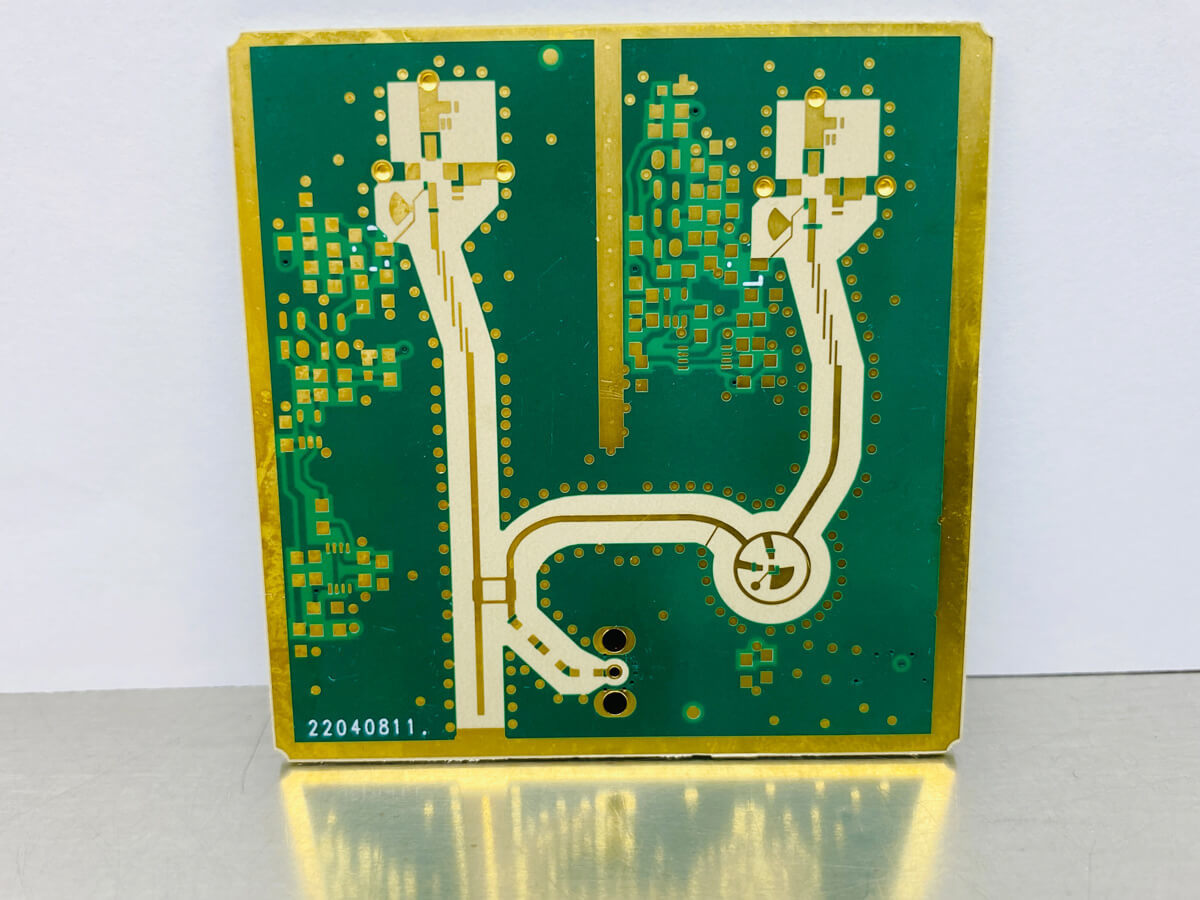
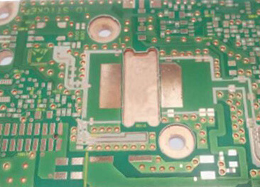
Type: Copper Substrate Category: PCB Manufacturing Thermal Conductivity: 1.0W/MK 1.2W/MK 1.5W/MK 2.0W/MK 2.4W/MK Surface Treatment: None Board Thickness: 1.5mm Outer Copper Thickness: 35um Type: Double-sided Copper Substrate Withstand Voltage: ≥4000 V TG: 170 Introduction: Aluminum substrates are mainly used in products with high thermal conductivity requirements, such as LED street lights and household energy-saving lamps. Copper substrates are mainly used in devices requiring fast heat dissipation and low expansion coefficients, such as military radars. Ceramic boards are mainly used in high-frequency base stations and automotive electronics.
Keywords: High-end productsmkcopperandin
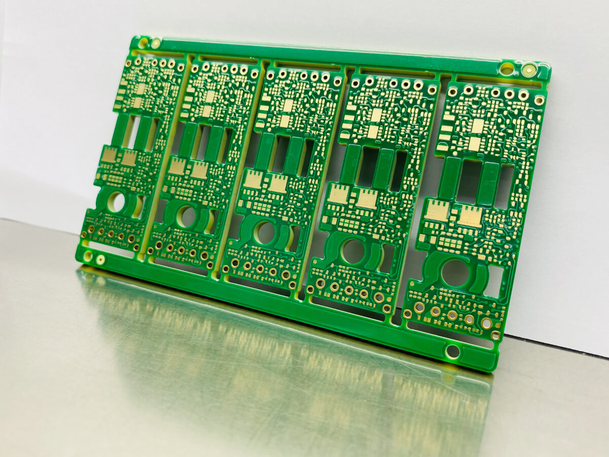
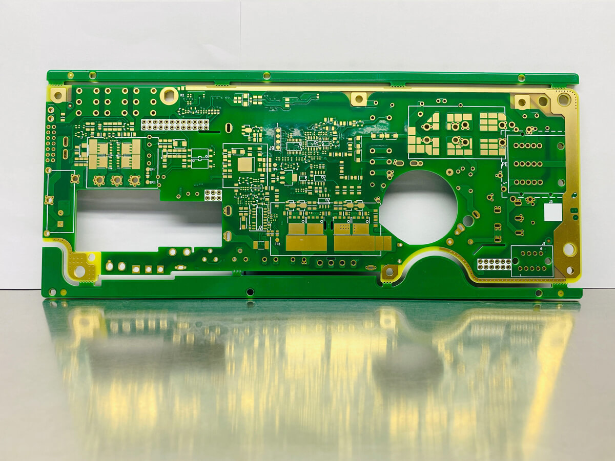
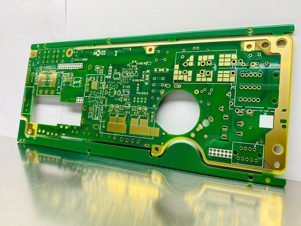
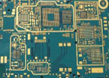
As the carrier of electronic components, the number of layers in a multilayer board and the precision of the circuit design determine the size and performance of the circuit board. This industrial-grade robot uses an 8-layer board design with 3 mil / 3 mil line width and spacing, and simultaneously packages 10 sets of ICs and 12 sets of BGAs, making it a high-end product of high-precision printed circuit boards. Main process features: ① Buried and blind via design; ② 3 mil line width and spacing; ③ BGA ball design requires uniform size and consistency; ④ IC green solder mask bridge 4 mil / 4 mil Process characteristics: high-precision interconnection board Technical specifications: 3 mil / 3 mil line width/spacing Finished board thickness: 2.0±0.1mm Outer copper thickness: 35um Surface treatment: immersion nickel gold
Keywords: High-end productsandofthemil